Wide-Band MEMS Microphones Application Guide
Microphone Placement within a Product
When designing a PUI Audio MEMS microphone into your product, careful PCB placement and sound hole position need to be considered to minimize noise. The microphone should be placed to avoid antennae, amplifiers, motors, power supplies, or any other devices that may create noise interference.
Additionally, microphones should not be placed on the same PCB as spring contact or surface mount speakers, as the vibration from the speaker is often transmitted to the microphone through the PCB, creating noise, echo, or feedback.
Microphone External Sound Hole Placement on a Product’s Housing
The external sound hole on a product should be limited in distance from, and larger in diameter than, the sound hole on the microphone.
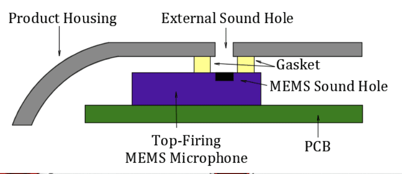
A direct path from the microphone’s sound hole (also referred to as the Acoustic Port) to the exterior of a product’s housing is required for optimum frequency response and to minimize unwanted noise from entering the microphone.
Placing the external sound hole on a flat surface simplifies the design of a gasket between the housing and the microphone sound hole.
Microphone Sound Channel Design
When designing the sound channel that connects the external sound hole to the microphone’s sound hole, first ensure that there is no leak by gasketing the area between the external sound hole and the microphone sound hole.
 |
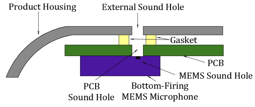 |
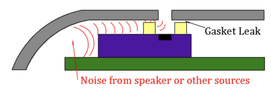
Many echo and feedback problems are caused by a leaky gasket between the sound hole between a top-firing microphone and the housing or between the bottom-firing microphone’s PCB and the housing. Please ensure the gasket is fully compressed to eliminate potential problems and/or a degradation in performance.
The sound channel should be kept as short as possible and larger in diameter than the microphone sound hole for top-firing microphones or be greater than or equal to the diameter of the PCB sound hole for bottom-firing microphones.
The diameter of gasket should be as close to the same size as the external sound hole to prevent creating a Helmholtz resonating chamber.
A long, thin or short, wide sound channel can “tune” the microphone, creating a peak in response between 10 kHz to 15 kHz, followed by a steep roll-off in frequency response thereafter.
Top-Firing Microphones: The diameter of the external sound hole and channel created by the gasket should be at least 0.1mm larger in diameter than the microphone’s sound hole.
Bottom-Firing Microphones: The diameter of the sound hole on the PCB should be at least 0.5mm to prevent solder paste from melting and entering the sound hole. Additionally, the interior of the PCB sound hole should not be plated to prevent solder paste from flowing into it.
Analog MEMS Microphone Circuit Design
Slight variances in power supply voltage do not affect the sensitivity of PUI Audio’s analog MEMS microphones (designated by AMM in the PUI Audio part number). As such, a circuit designer only needs to ensure that the voltage output of the power supply is within the voltage range called out in the MEMS microphone specifications.
Unlike traditional ECM microphones, MEMS microphones do not require the use of a bias resistor between the power supply and the microphone. MEMS microphones have an independent output that is separate of the voltage input. It is recommended to decouple the noise of the power supply from the MEMS microphone by using a 0.1µF capacitor at C1 in the diagram below.
A DC-blocking/high-pass filter capacitor should be placed between the MEMS output pin and the CODEC/ADC/pre-amplifier’s input pin, C2 in the diagram below. Values between 1µF and 3µF are often used, where the larger the capacitor value, the higher the frequency at which the high-pass filter’s corner frequency is placed.
In the event of electro-magnetic interference, place a resistor that matches the microphone’s impedance between the amplifier’s unused differential input and the microphone’s ground.

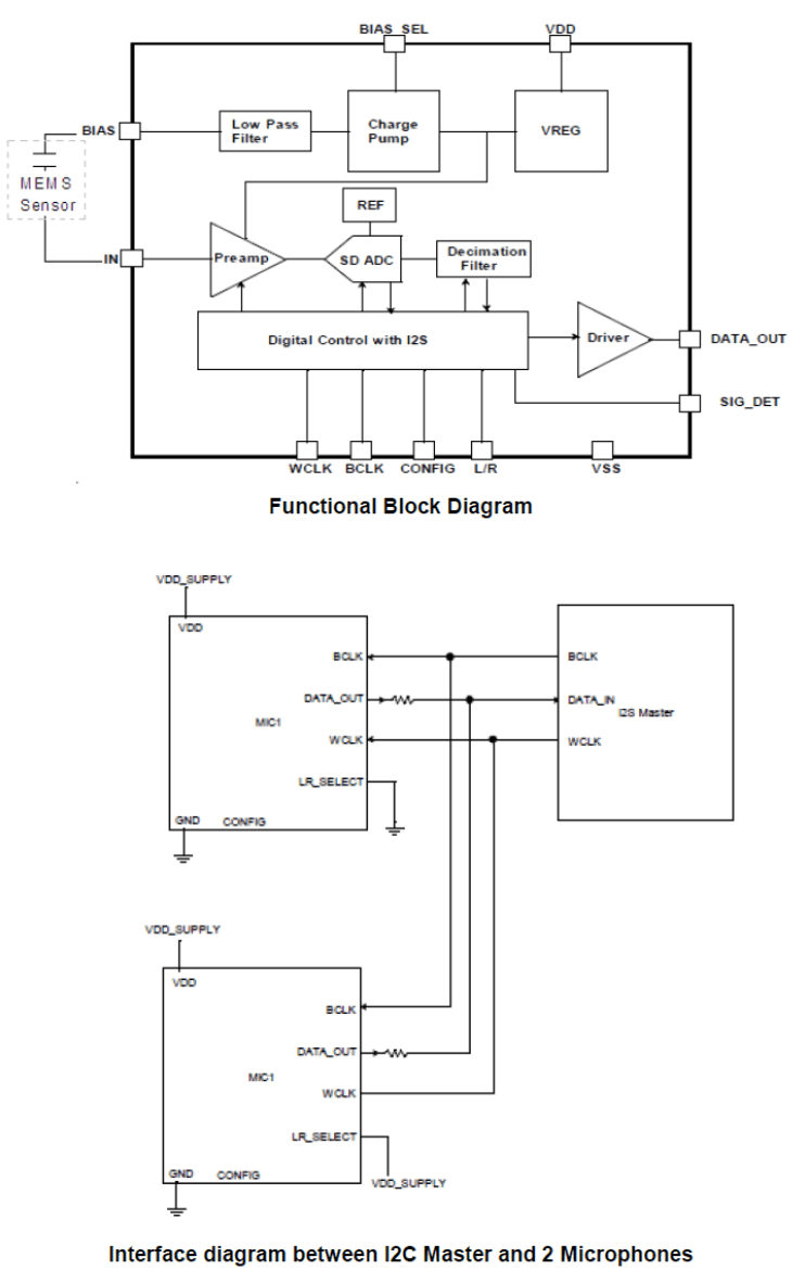
Digital MEMS Microphones
PUI Audio offers digital output MEMS microphones (designated by DMM in the PUI Audio part number) with PDM and I2S data formats. Both feature a Left/Right channel select pin for stereo audio capture and data transfer over a single data input line on a DAC or CODEC. The I2S digital MEMS (DMM-4026-B-I2S-R) microphone also offers the ability to set up microphone arrays by changing the WCLK Hold Time.
PUI Audio’s digital MEMS microphones offer a Full Power mode, a reduced sensitivity Low Power mode, and a Sleep mode for reduced current draw and battery powersavings when the microphone isn’t needed.
Modes are activated by changing the input clock frequency to the microphone.
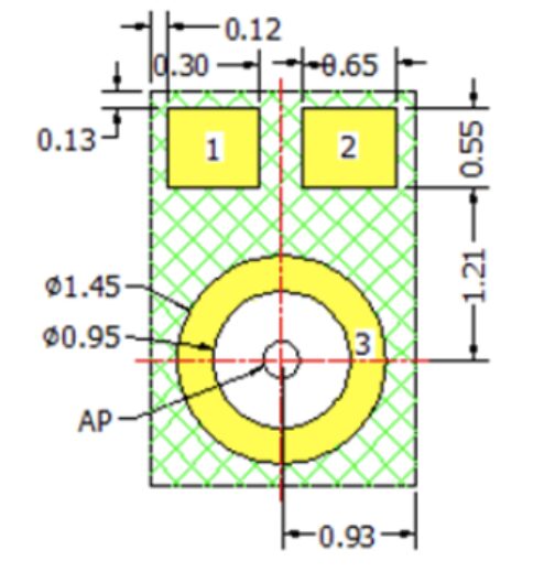
Solder Pad and Stencil Design
Each MEMS microphone is built for reflow soldering, where the solder joints serve as the means for electrical and mechanical connection to the PCB. On bottom-firing microphones, a solder joint also acts as the acoustic seal between the microphone sound hole and the PCB.
The recommended solder pad design and stencil layout is listed within the specifications for each microphone. The PCB solder pad to microphone pad ratio is 1:1
 |
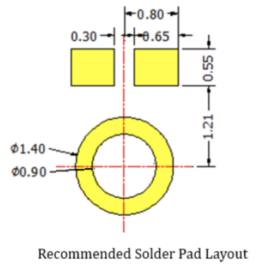 |
Solder Paste
A Type 4 no-clean solder paste is recommended to be used with PUI Audio’s MEMS microphones. The stencil thickness should be between 0.1mm to 0.12mm, with the ratio of the size of the stencil to pad being between 0.8:1 to 0.9:1 to minimize tin bead content.
For bottom-firing microphones, solder pastes with low flux content (such as Indium 8.9 HF SAC305) are recommended to prevent excessive flux from entering the microphone sound hole, causing damage.
 Pick-and-Place Operations
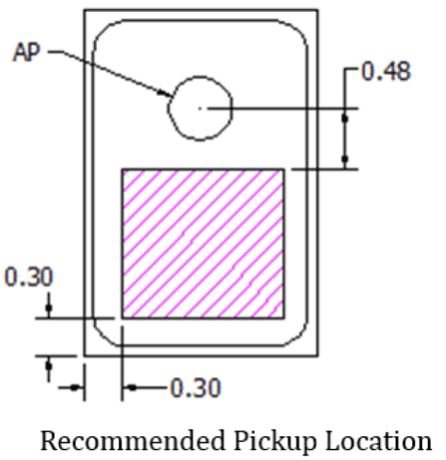
Special attention needs to be observed when programming an SMD pick-and-place machine (also known as P&Ps) to place top-firing MEMS microphones (designated with a –T within PUI Audio’s part number) due to the placement of the sound hole (referred to as the Acoustic Port or AP in the specifications) on the same surface that vacuum is applied to.
The specifications call out the recommended pickup location, and the location of the sound hole. To avoid damaging top-firing microphones, do not allow the SMD pickup nozzle to pass over the sound hole. The inside diameter of the nozzle must only move directly to the recommended pickup location, which is pink in the PUI Audio specifications.
Programming the SMD pick-and-place machine to place bottom-firing microphones is easier as the sound hole is placed on the bottom of the part.
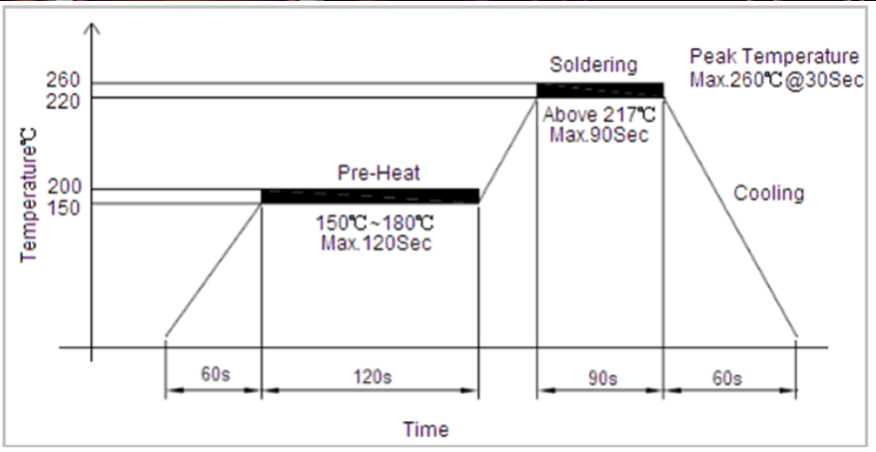 Reflow Soldering
PUI Audio’s MEMS microphones feature gold-plated pads for lead-free reflow soldering. Please follow the reflow process below and do not exceed a total of three cycles. If multiple reflow cycles are required, the microphone must be allowed to return to room temperature before the start of the next reflow cycle.
Allow the microphone to rest at room temperature for a minimum of three hours before functionally testing it.
MEMS Microphone PCB Cleaning Considerations
On PCBs that contain a PUI Audio MEMS microphone, please follow these precautions to minimize potential damage to the microphone.
- Do not wash or clean PCBs after the reflow process.
- Do not expose the PCB to ultrasonic processing or cleaning.
- Do not pull a vacuum over the microphone sound hole (on both top-firing and bottom-firing microphones).
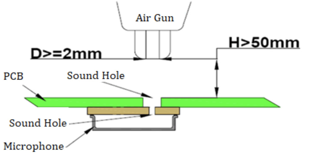
- Do not apply more than 0.3mPa of air pressure into the microphone sound hole.
- If a dust removal system is used, please ensure that the air gun nozzle diameter is greater than or equal to 2mm, less than 0.3mPa of air pressure is used, the distance between the tip of the air gun nozzle and the PCB is greater than 50mm, and that the total cycle duration is less than five seconds.
- To eliminate the chance of dust entering the microphone’s sound hole, it is recommended that the sound hole be covered during the dust removal process, if possible.